

EMC/EMI Course Syllabus

Introduction to EMC
- Background terms and definitions
Commercial and Military Standards on EMC
- Brief description of the Purpose and intent of the standards, with focus on those requirements which are difficult to meet

Spectrum and time domain signals
- Spectrum of communication data signals, clocks and switching mode power supplies.
- Engineering aspects of the parameters which often cause failures in EMC Compliance testing
Cables in EMC: as radiators and as radiation receptors
Switched Mode power supplies
- Sources of interference in switched mode power supplies-SMPS,
- Identification of the generators of interference and their control, filtering an SMPS to comply with the requirements of conducted Emissions on the power leads.
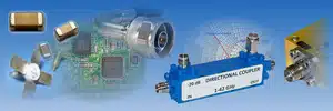
Filtering of conducted interference
- Principles of EMI Filtering,
- Structure and topology of common filters,
- Limitations of filtering components,
- Selection of a filter based on termination impedances and filtering requirements.
- Filtered pin connectors.
- The importance of the placement of the filter,
- Considerations when selecting or designing a filter
Shielding
- The need for shielding,
- Materials used for shielding,
- Properties of metals conducive to shielding,
- Basic shielding theory,
- Engineering results as to the materials to be used,
- Shielding integrity faults due to penetrations and apertures and how to control them, engineering results as to bolt spacing.
- Cable shielding, gaskets, vents, viewing ports
Transients
- Sources of transients,
- Expression for transient immunity in the standards for lightning,
- Inductive load switching and ESD.
- Selection of TVS transient voltage suppressor components to comply with the standards
Grounding
- Purpose of grounding,
- Impedance of conductors used for grounding,
- Single and multiple point grounding,
- Hi speed board grounding
Bonding
- Bonding for electrical continuity,
- Electro-chemical properties of metals, corrosion effects, surface treatment to avoid corrosion,
- Bonding resistance requirements
EMC aspects of Electronic Circuit Design
- Selection of electronic component technology to minimize conducted and radiated Emissions.
- Board design for component placement, layer stack-up, separation of traces, area segregation in ground and power planes,
- Pin allocation in board to mother board connectors,
- On board filtering
Preparedness for EMC Lab testing
- The requirements of the standards,
- The EMC Test Plan,
- Setting the modes of operation, setting the pass-fail criteria, separation between the equipment being tested and the associated controlling-operating equipment
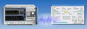
Spectral Analysis
- Signals in time and Frequency Domain
- Types of Spectrum Analyzers
- Basic Block Diagram of an Analog SA
- The SA as a Receiver
- Selectivity, AGC, LO Phase Noise
- Microwaves Spectrum Analyzer
- Frequency Resolution and RBW
- Limitations on the Sweep Rate
- RF Attenuator
- IF Amplification
- Shape Factor of the RBW Filter and Sweep Rate
- Noise Floor
- Video Signal Filtering (Post-Detection)
- Filtering by Averaging Screens
- SA Controls (Span, RBW, Att, VBW)
- Dynamic Range
- Detector Types and their Characteristics
- Sampling and the Sampling Theorem
- Spectrum of a Uniformly Sampled Signal
- Artifacts in Digitally Processed Spectrum Display
- Side-Lobes in Frequency Domain and Windowing
- RBW broadening by Windowing
- 2nd and 3rd Order Distortions and Spurii – Identification of Saturation in the SA
- Effect of LO Phase Noise
- Residual FM
- Time Domain Measurements – Zero Span
- Signal Power response in time
- Intermodulation Measurements
- Intermodulation with two-tones Stimulus
- Adjacent channel power (ACP)
- Adjacent channel leakage ratio (ACLR)
- Tracking Generator Configuration and Scalar Network Analyzer Measurements
- Demonstration of SA operation and Measurements
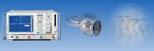
Vector Network Analyzer
- Introduction to the Network Analyzer
- Measurement Types Performed by the VNA
- Scalar and Vector Network Analysis
- Review of Transmission Lines
- Transmission and Reflection Parameters
- S parameters
- Construction of the VNA
- Coupling to the Measured Signals
- Detection Types
- Dynamic Range
- T/R Setup versus S-Parameters Measurements
- Types of Measurements Errors
- Basic Error Models and Calibration
- One-Port and Two-Port Models
- Review of Calibration Methodologies for Minimization of Errors
- Measurements Review – Power Sweep for AM/AM, AM/PM, and Harmonics
- Time Domain Measurements (TDR)
- Demonstration of VNA operation and Measurements
EMC/EMI Simulation using the CST EMC STUDIO® software
- Solver Choice for EMC Applications
- Basic Meshing
- Circuit and 3D System Level Simulations
- Workflow examples:
- Conducted Emission: DC DC Converter
- Panel Shielding Effectiveness
- Lightning Strike Simulation
- Electro Static Discharge (ESD)
- USB Example: Cascading
- Conducted Emission: DC DC Converter
- Radiated Emission
- Rule based EMC checking

Fundamentals of PCB design for Power and Signal Integrity and EMC Compliance
- Signal Integrity, Power Integrity and EMC compliance – Challenges to the Electronic designer
- Characteristics of PCB as a medium of high speed signals
- 3D structure of signal transfers between layers
- Preparation for layout and layout considerations
- Designing Layers order according to project requirements
- Distribution of layers contents according to multi voltages circuit
- Options for implementing the order of layers to comply with EMI requirements
- Calculating the final thickness of a circuit to meet mechanical requirements
- Proper planning of the order of the layers – the rules of the copper balance
- Considerations in components layout in Mixed Signals Design
- Effective physical location of the PCB termination components
- Table of recommendations and reasons for choosing a type of termination according to LOGIC
- Knowledge of signals characteristics according to the electronic classification of the groups
- Priority considerations for routing between lead groups
- Basic rules in conductor routing
- Routing CLOCK, Tree, Daisy-Chain, Stubs
- Considerations in the routing of data and ADDRESS bus
- Routing CONTROLLED IMPEDANCE lines
- INPUT / OUTPUT conductors Insulation
- Rules for Differential-Pair routing according to the frequency
- Split according to technology RF/ANALOG/DIGITAL
- The effect of a signal transition over splitting surfaces POWER/GROUN
- Common errors that affect IMPEDANCE planning
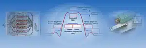
Military EMI Control standard for Equipment
- Mil Std 461G history, structure, basic requirements for lab facility, scan of the testing requirements, the purpose, rationale and limits. Tailoring of the standard limits
Commercial EMI Control standards for Equipment
- FCC part 15 limits on conducted and radiated emissions.
- The difference between class A and Class B ITE,
- The meaning of a Quasi Peak limit.
- European community- CE EMI control standards,
- Emissions and susceptibility.
- The open area test site-OATS and its shielded enclosure replacement.
- Failure criteria.
- Scan of the immunity requirements per EN61000-4.
An Introductory tour in Hermon Labs
An Introductory tour in Hermon Labs to acquire familiarity with the environment and testing methods